PVD (Physical Vapor Deposition) coating is one of today’s finest surface treatment technologies and is very adaptable to many of industrial manufacturing processes. Moreover, with recent industrial demands for coatings that are thinner and harder, with less environmental impact, PVD technology has progressed (from an aerospace niche application) to an accepted form of manufacturing for the automotive, medical, electronic, and decorative industries.
Therefore, engineers, purchasing agents, and product designers who work with surface treatments should have a good understanding of PVD coating, how it functions, and why it outperforms other surface technologies.
Let’s dive deeper into every aspect of PVD coating, including specification, qualification, and optimization for precise manufacturing. This guide will cover everything from vacuum physics to criteria for selecting a coating so that you can make technically sound decisions.
What Is PVD Coating?
PVD (Physical Vapor Deposition) is a group of techniques to produce thin films using a solid source material that is vaporized in a vacuum and condensed back into the solid state on a substrate surface. PVD only uses solid-to-vapor-to-solid transitions and has no liquid chemicals or chemical reactions that occur during deposition, as electroplating does.
As a result, the deposited thin films exhibit metallurgical bonding (like welding) to the substrate instead of just mechanical or chemical bonding. Coating thicknesses for PVD are normally between 0.25 microns (µm) and 5 µm; however, certain specialized multilayered structures can be much thicker. At this scale, the deposited coating becomes an engineered functional material and not just a coating.
The PVD process is performed in a high vacuum chamber at pressures of 10⁻² to 10⁻⁶ Torr (approximately the same as the atmospheric pressure in low Earth orbit); hence, the vaporized atoms travel in a straight line towards the substrate with very few collisions while they are still in the gas phase (before impacting on the surface).
PVD Coating vs. Other Surface Treatment Technologies
To better appreciate the worth of PVD coating, it can be useful to compare it directly to some other coating options that engineers commonly evaluate:
| Parameter | PVD Coating | CVD Coating | Electroplating | Thermal Spray |
| Process Temperature | 150–500°C | 500–1100°C | Room temp (aqueous) | 1500°C+ (flame) |
| Film Thickness | 0.25–5 µm | 1–25 µm | 1–1000 µm | 50–500 µm |
| Adhesion Mechanism | Metallurgical bond | Diffusion bond | Electrostatic/chemical | Mechanical anchoring |
| Hardness (typical) | 1500–3500 HV | 1500–3500 HV | 100–600 HV | 400–1200 HV |
| Toxic By-products | None (inert gas) | Yes (HCl, HF, etc.) | Yes (heavy metals) | Variable |
| Substrate Distortion | Very low | High (temp effect) | Low | Moderate–High |
| Line-of-Sight Limit | Moderate | None (conformal) | None (conformal) | Yes (direct only) |
As shown in the table, PVD coating provides a unique combination of extreme hardness, metallurgical adhesion, and zero toxic waste that no other coating process (i.e., electroplating and CVD) can match at the same time.
How the PVD Coating Process Works?
The PVD coating process includes many systematic methods. Each of these processes has a direct impact on the overall characteristics of the coating, including the microstructure, adhesion properties, and performance. By understanding these processes, a coating engineer can specify the correct parameters to produce a satisfactory coating with fewer complications.
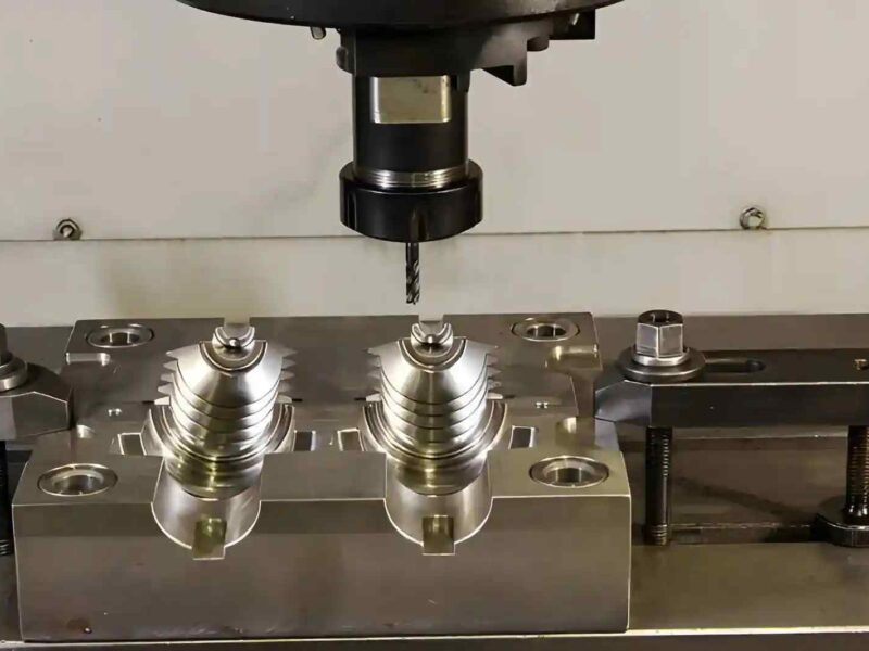
Step 1: Substrate Preparation and Cleaning
Prior to applying a deposit to a substrate, the surface of the substrate undergoes rigorous cleaning and preparation. This involves alkaline ultrasonic cleaning solutions or cleaning chemicals to dissolve any contaminating materials or residues from the substrate. After ultrasonic cleaning, the substrate surfaces are rinsed with water and dried. After receiving ultrasonic cleaning, substrates usually undergo in-situ plasma cleaning in a vacuum chamber with an argon ion beam at 400 to 800 eV. Any remaining oxides or contaminants on the substrate prior to depositing a PVD coating will inhibit the ability of the coating to bond to the substrate. However, the substrate is not clean; even the most advanced PVD coating equipment will produce coatings that will delaminate during service.
Step 2: Chamber Evacuation
The coated components are placed in a stainless steel vacuum chamber that is depressurized to base pressures ranging from 10⁻⁵ to 10⁻⁶ Tor. Explore this using a combination of rough pumps and turbomolecular pumps to create a vacuum that is free from air, moisture, and other impurities. This step is crucial because these impurities can contaminate the growing film or scatter the vapor stream. The substrate is frequently heated to temperatures between 150 °C and 500 °C by radiative means. This heating promotes the enhancement in the movement of adatoms and the crystallization of the film.
Step 3: Vaporization of the Target Material
The target material is vaporized using one or more of several different methods of energy input. The vaporized target material (as atoms or ions) travels through the vacuum chamber in a nearly collision-free manner and strikes the substrate after traveling this distance with kinetic energy between 1 and 100 eV, depending upon the type of PVD method employed.
Step 4: Film Nucleation and Growth
When the vapourised elements reach the heated substrate, they will begin to nucleate at sites on the surface and then proceed to grow epitaxially or polycrystalline, depending on the temperature of the substrate, the rate of deposition, and the working pressure. During the final stage of coating development, it is standard to introduce reactive gases such as nitrogen, oxygen, or acetylene into the sputtering process to form compound coatings. One example of a compound coating is Titanium Nitride (TiN), which is formed by the reaction between vapourized titanium and nitrogen. The use of reactive gases in the PVD process enables the direct formation of nitrides, oxides, carbides, and oxynitrides during deposition.
Step 5: Post-Deposition Cooling and Quality Inspection
After the deposition of the coating, the chamber is fully backfilled with an inert gas, and the parts are allowed to cool before extraction. The inspection of the coatings includes several techniques, including Hardness testing (Vickers or nanoindentation), adhesion testing (Rockwell or progressive Load Scratch testers), thickness measurement (calotest or X-ray fluorescence), and surface roughness measurement (profilometry). Therefore, all batches can be thoroughly tested prior to being sent into manufacturing.
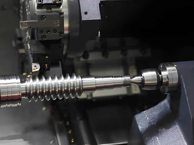
Types of PVD Coating Processes: Sputtering, Arc Evaporation, and More
There are several different ways to apply a PVD coating. Each of these coatings can have different structures and deposition methods. PVD process type will also affect properties of a coating, such as density, ionization level, deposition rate, and material compatibility with the substrate. The three major industrial PVD processes are: Magnetron sputtering, Cathodic Arc, and Thermal/Electron Beam.
1. Magnetron Sputtering
In magnetron sputtering, a magnetic field is placed over a DC or RF electrical discharge to keep electrons near the surface of the target. This significantly increases the amount of plasma, and consequently, the number of atoms ejected from the target during sputtering. The argon ions, which have been accelerated by the electric field, strike the target with energies between 200 eV and 1000 eV and eject target atoms that travel to the substrate. DC magnetron sputtering is appropriate for conductive targets (metal and alloy), while RF sputtering is appropriate for insulating materials (ceramic and oxide).
Due to the ultra-smooth surface and uniformity of sputtered films Ra < 0.1 µm), magnetron sputtering is the most commonly used PVD process for optical coatings or decorative PVD finishes, or for metallization of semiconductors. Furthermore, you can combine sputtering with a reactive gas (N2 or O2) to create, in one deposition step, a functional hard coating (TiN, CrN, AlTiN, etc) on a target.
2. Cathodic Arc Deposition (Arc PVD)
Cathodic Arc PVD works by establishing a high-current, low-voltage electrical arc (usually between 50-150 A and 20-30 V) that rapidly travels over the surface of a target (starting point for depositing material). The rapid movement creates numerous localized micro-spots on the surface of the target from where material is vaporized in an instant (to create a highly ionised (over 90 %) plasma. The result is that all of the depositing species have a great deal of kinetic energy. Thus, they penetrate deep into the surface of the substrate, creating extremely dense and well-adhered coatings (> 3000 HV hardness).
However, the application of cathodic arc coatings creates macroparticles (i.e., micron-sized, molten droplets created when the arc strikes a molten spot). These droplets can slightly roughen (i.e., cause surface roughness) the film surface. In tooling applications where adhesion and hardness are critical, cathodic arc PVD is best. In optical or decorative applications that require mirror-smooth surfaces, filtered arc PVD or sputter deposition is best.
3. Thermal and Electron Beam Evaporation
Thermal evaporation heats the source (e.g., tungsten filament, boat, crucible) to an evaporation temperature through a resistive heating method under vacuum. Electron beam evaporation performs the same function as thermal evaporation by using 10–15kv focused electron beams instead of resistive heaters to evaporate high-melting-point sources; for example, tungsten (3422 degrees C) and molybdenum. Both methods yield far less ionization than arc PVD (<5%); therefore, the evaporated atoms impact the substrate at low energy (generally 0.1–1 eV), resulting in lower coating density compared to arc PVD. Nevertheless, evaporation provides the ideal method for pure metal coatings, optical thin films (MgF₂, SiO₂, ZrO₂), and microelectronics contacts due to its high purity characteristics.
| PVD Method | Ionization Level | Deposition Rate | Film Smoothness | Best For |
| DC/RF Magnetron Sputtering | 10–40% | 0.1–1 µm/min | Excellent (Ra <0.1 µm) | Decorative, optical, semi-conductors |
| Cathodic Arc Deposition | >90% | 1–10 µm/min | Good (Ra 0.1–0.3 µm) | Hard tooling, wear coatings |
| Thermal Evaporation | <5% | 0.01–1 µm/min | Excellent (Ra <0.05 µm) | Optical films, electronics |
| Electron Beam Evaporation | <10% | 0.1–5 µm/min | Excellent (Ra <0.05 µm) | Refractory metals, aerospace TBCs |
| Ion Plating (HiPIMS) | 50–90% | 0.05–0.5 µm/min | Very good | Dense functional coatings, R&D |
Common PVD Coating Materials and Their Technical Properties
The functional performance of PVD Coatings depends upon the base properties of the Coating Material and the Stoichiometry achieved during Deposition. Therefore, Material Selection is arguably the single most important Engineering decision in the total specification of the PVD Process.
| PVD Coating | Hardness (HV) | Max Service Temp (°C) | Friction Coeff. (dry) | Color | Key Applications |
| TiN (Titanium Nitride) | ~2000 | ~600 | 0.40–0.55 | Gold/Yellow | Cutting tools, medical devices, decorative |
| TiCN (Titanium Carbonitride) | ~3000 | ~400 | 0.20–0.35 | Grey-violet | High-speed steel tools, forming dies |
| TiAlN (Titanium Aluminum Nitride) | ~3200 | ~800 | 0.35–0.55 | Dark violet | Dry-cutting, aerospace, high-speed milling |
| AlTiN (Aluminum Titanium Nitride) | ~3300 | ~900 | 0.30–0.50 | Black-grey | Hard milling, hardened steels |
| CrN (Chromium Nitride) | ~1750 | ~700 | 0.30–0.40 | Silver-grey | Injection molds, hydraulics, marine |
| ZrN (Zirconium Nitride) | ~2200 | ~550 | 0.35–0.40 | Light gold | Decorative (watch components), food industry |
| DLC (Diamond-Like Carbon) | ~3500 | ~400 | 0.05–0.15 | Black | Automotive bearings, medical implants, optics |
| CrAlN (Chromium Aluminum Nitride) | ~3000 | ~1100 | 0.30–0.40 | Dark grey | Turbine blades, high-temp tooling |
To date, the two dominant choices for high-performance Cutting Tool Coatings are TiAlN and AlTiN. Both of which will develop an Al₂O₃ alumina Protective Layer when exposed to elevated temperatures. Thus, they will provide a thermal barrier and considerably increase the cutting life of Cutting Tools in Dry and Semi-Dry machining applications. Conversely, DLC Coatings continue to receive significant R&D Investment from the Automotive and Biomedical Industries, because of their uniquely low Coefficient of Friction and their excellent Biocompatibility.
Industrial Applications of PVD Coating
PVD coatings have found their way into nearly every type of precision manufacturing. Each of the coatings serves a different purpose to solve a problem that traditional bulk material selection or heat treatment cannot solve.
Cutting Tools and Tooling
The cutting tool industry is still the largest global market for PVD coating consumption. TiN, TiCN, and TiAlN coatings on carbide and high-speed steel end mills, drills, inserts, and taps can increase the life of these tools by 200%-500% compared to non-coated equivalents. In addition, the coatings’ low coefficient of friction decreases the cutting forces and adhesion of chips during cutting, allowing for greater speed and better quality of the finished product.
Aerospace and Defense
Aerospace PVD coatings need to meet very high demands of thermo-mechanical performance. Coatings that use CrAlN and AlCrN will provide protection for turbine blade root sections from fretting fatigue and oxidation, up to 1100°C. Coatings of DLC on actuator components and bearing races reduce the weight penalty of using lubrication systems (which are much heavier), while providing ultra-low wear rates during severe oscillatory contact conditions.
Medical Devices and Implants
The medical implant sector benefits from the application of PVD coatings due to their biocompatibility, sterilization, and/or corrosion resistance. Historically, titanium nitride (TiN) has been established by the FDA as a biocompatible material used for coating orthopedic implants and surgical instruments. DLC coatings applied to femoral heads of hip implants produced wear rates ranging from 0.1 to 0.55 mm3/million cycles (simulated testing), which is approximately 10 times lower than uncoated CoCrMo. Additionally, PVD processes produce zero toxic residues, thus meeting the stringent biocompatibility requirements established by ISO 10993 for Class III implantable devices.
Consumer Electronics and Semiconductors
PVD technology is an essential part of the production of all types of semiconductors. It is used extensively in the creation of diffusion barriers (i.e., TiN and TaN), seed (i.e., Cu and Ru), and contact metals (i.e., W, Ti, and Co) deposits on silicon wafers. PVD processing occurs at substrate temperatures <200ºC to avoid thermally damaging the transistor junctions created prior to this process. High-ionization (e.g., HiPIMS) PVD processes provide the ultra-conformality necessary to line high-aspect-ratio vias and trenches without voids as the semiconductor process shrinks below a 5 nm node size.
Automotive Components
PVD applications for automotive products include improving the performance of competitively priced and environmentally compliant combustion engines. The reduction in friction coefficient of ~0.12 (uncoated) to ~0.05 (coated with DLC) achieved by using DLC-coated piston rings translates to fuel efficiency improvements of up to 5% in combined cycle performance testing. Other benefits of using PVD-coated piston rings and valve train components include corrosion resistance when operating on ethanol-blended fuels and acidic products of combustion.
PVD Coating vs. CVD Coating: Which Should You Specify?
When choosing between hard coatings for cutting tools, engineers often weigh the benefits of Physical Vapor Deposition (PVD) vs Chemical Vapor Deposition (CVD). That’s because although coating materials are similar, processes differ significantly for the purposes of coating material application.
The CVD process vaporizes materials in the gas phase and then deposits coatings at a temperature in the range of 900 to 1100ºC. And since the coating process occurs at this high temperature, it allows coatings to firmly adhere to complex geometries such as those that are re-entrant (curved in) and allows for thick Al₂O₃ coatings, which have an excellent performance in crater wear resistance when cutting steel. Finally, the deposition temperature of CVD can create residual tensile stress within the coating, which will, in turn, create structural (decarburization) changes in the carbide substrate, which can reduce the transverse rupture strength of the substrate by as much as 15-30%.
On the other hand, PVD coatings are deposited at temperatures between 150 and 500ºC, which creates residual compressive stress in the coating, enhancing their performance in interrupted cutting operations and applications where high impact loads are present, such as milling and drilling operations. In addition, PVD coatings can be universally applied to high-speed steel (HSS), cermet, and fine-grained carbide substrates, which cannot tolerate the extreme temperatures of the CVD process. Therefore, the PVD coating method is the preferred choice for milling, drilling, threading, and all applications requiring interrupted cutting.
Final Verdict
PVD Coatings are functionally different from many surface finishes due to their precision engineering at the atomic level. The process of PVD Coatings produces an exceptional level of hardness (up to 3500 HV), metallurgically bonded to the substrate with thin films of coating (0.25–5 µm). The method has the capability to operate at temperatures as high as 1100°C, and is totally clean and waste-free during production.
At Premium Parts, we produce precision components with PVD Coatings to meet stringent dimensional, functional, and regulatory specifications. Whether you need to have TiAlN coating for aerospace parts or CrN-coated hydraulic components, our engineering team will help, from selecting the substrate to performing the final inspection.
If you would like to discuss any of your PVD Coating requirements or would like to schedule a technical consultation with Premium Parts, please contact us today.